The FilmTek™ 2000M TSV is a fully automated, non-destructive metrology tool that uses highly collimated light at normal incidence to measure film thickness, critical dimension (CD), total thickness variation (TTV), high-aspect-ratio trenches, and through-silicon via (TSV) applications in both front-end and advanced packaging development. 2000M TSV is useful for high-volume semiconductor manufacturing, MEMS foundries, R&D, and shared common development facilities because of its adaptability and broad application coverage in a single platform.
FilmTek 2000M TSV delivers
- High-resolution detector/spectrometer with nanometer resolution that can resolve extremely high-frequency oscillations from thick films.
- Due to patented signal collection and post-processing, a broad range of thickness measurements from 5 nm to 350 μm, even on rough metal substrates, are possible.
- Tiny spot sizes as little as 2 × 1 μm make it possible to measure high aspect ratio (HAR) vias or films in constrained spaces.
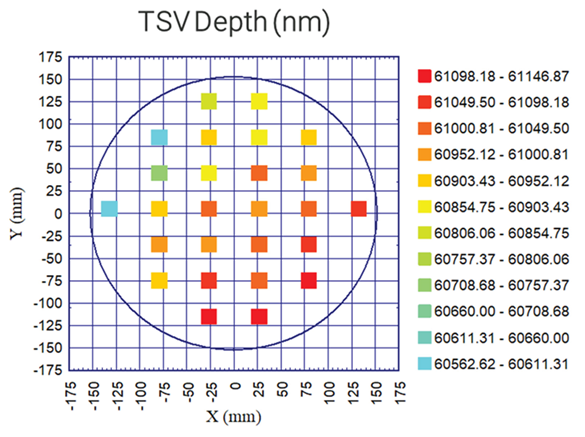
26-point patch plot of TSV depth variation across a 300 mm wafer. Image Credit: Bruker Nano Surfaces
Delivering application flexibility
Film thickness measurements using a patented optical design for collimated light
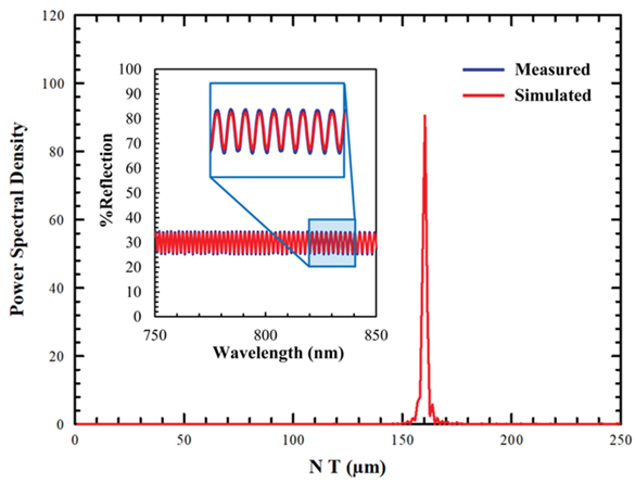
Power spectral density (PSD) plot that enables fitting to yield improved thickness accuracy and repeatability. Inset: Measured and simulated reflectance spectra of ~100 μm photoresist on silicon, showing high frequency oscillations. Image Credit: Bruker Nano Surfaces
Standard reflectometry techniques use a highly concentrated light beam to produce a small measurement spot size. For thick film applications, a concentrated beam with a high numerical aperture will gather a broad range of reflected angles, leading to destructive interference and incoherent reflectance.
The patented optical design of the FilmTek 2000M TSV produces a collimated beam with a small spot size, enabling coherent measurements of both thick and thin films. Accurate thickness measurements from 5 nm to 350 μm with 2000M TSV are possible with coherent reflectance maintained for thick films with a collimated beam and small spot size. The high-frequency oscillations frequently seen in the reflectance data can be fitted and modeled by 2000M TSV when used in conjunction with a high-resolution spectrometer for thick films.
High aspect ratio TSV characterization using non-destructive reflectance measurements
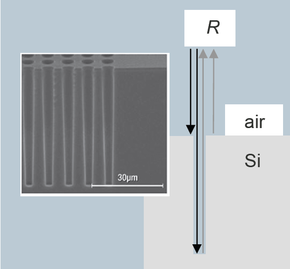
Schematic and scanning electron microscope image (inset) of HAR TSV structures. Image Credit: Bruker Nano Surfaces
The Filmtek 2000M TSV characterizes HAR TSV structures using a patented optical design and processing method through quick and nondestructive reflectance measurements. The optical design of 2000M TSV avoids this issue by using a collimated beam and adjustable spot size to provide consistent, coherent reflectance data from HAR TSV structures. Conventional reflectometry systems are unable to reliably measure TSV depth due to incoherence.
The CCD camera can be used to measure the top CD of the TSV and for other imaging applications, while the high-resolution spectrometer is designed to measure the depths of TSV structures based on light reflected from the top and bottom of the TSV. It is possible to measure TSV diameters with aspect ratios of 40:1 with accuracy as small as 2 μm.
Simple reflectance measurements can provide comprehensive real-time results for TSV depth and CD analysis using patented TSV data processing methods.
Small-spot measurements for next-gen semiconductor applications
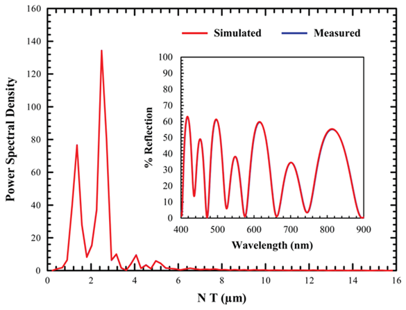
PSD plot of 500 nm Si3N4 on 950 nm SiO2 on an Si substrate, showing a distinct peak from each layer. Inset: measured and simulated spectra the SiN/SiO2 stack, measured with a 2 μm spot size. Image Credit: Bruker Nano Surfaces
2000M TSV’s patented optical design enables manufacturers to stay ahead of the curve with a variable spot size that can go as small as 2 × 1 μm, capable of measuring the smallest test pads and in extremely tight spaces, while the semiconductor industry continues to find innovative ways to produce smaller devices. 2000M TSV can measure thin and thick layers on top of and around devices to provide process control and reduce scrap in various applications, including front-end manufacturing, sophisticated packaging, and hard drive applications.
How small-spot collimated-beam technology works
A white light beam is directed through a microscope using beam splitters after being collimated by a variable aperture. Different objective lenses, both high and low, are used to achieve different spot sizes, down to 2 × 1 μm. On the XYZ stage, the collimated beam exits the objective normal to the sample. After reflecting off the sample, the beam enters the lens through a second beam splitter. A high-resolution spectrometer receives one portion of the beam that passes through a pinhole slit, and a CCD camera receives the remaining portion that provides a real-time view of the measurement site.
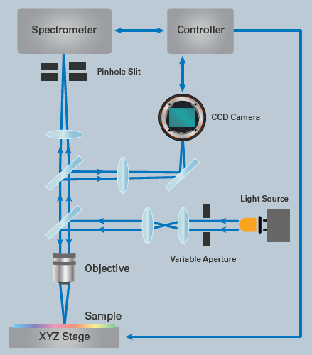
Image Credit: Bruker Nano Surfaces
FilmTek 2000M TSV specifications
Source: Bruker Nano Surfaces
| . |
. |
| Measurement function |
TSV etch depth, bump height, critical dimension, and film thickness |
| Wafer handling |
Brooks or Bruker’s internal handling solutions |
| Substrate size |
200 or 300 mm |
| Pattern recognition |
Cognex |
| CD precision (1σ) |
<30 nm |
| Etch depth precision (1 σ) |
<10 nm |
| Film thickness range |
5 nm–350 μm (5 nm–150 μm is standard) |
| Film thickness precision (1 σ) |
<1 nm |
| Spot size |
10x: 5x10 μm²; 20x: 2.5x5 μm²; 50x: 1x2 μm² |
| Light source |
Halogen lamp |
| Detector type |
2048-pixel linear CCD array |
| Wafer throughput |
>40 WPH; 17-point map |